What is PCB design software?
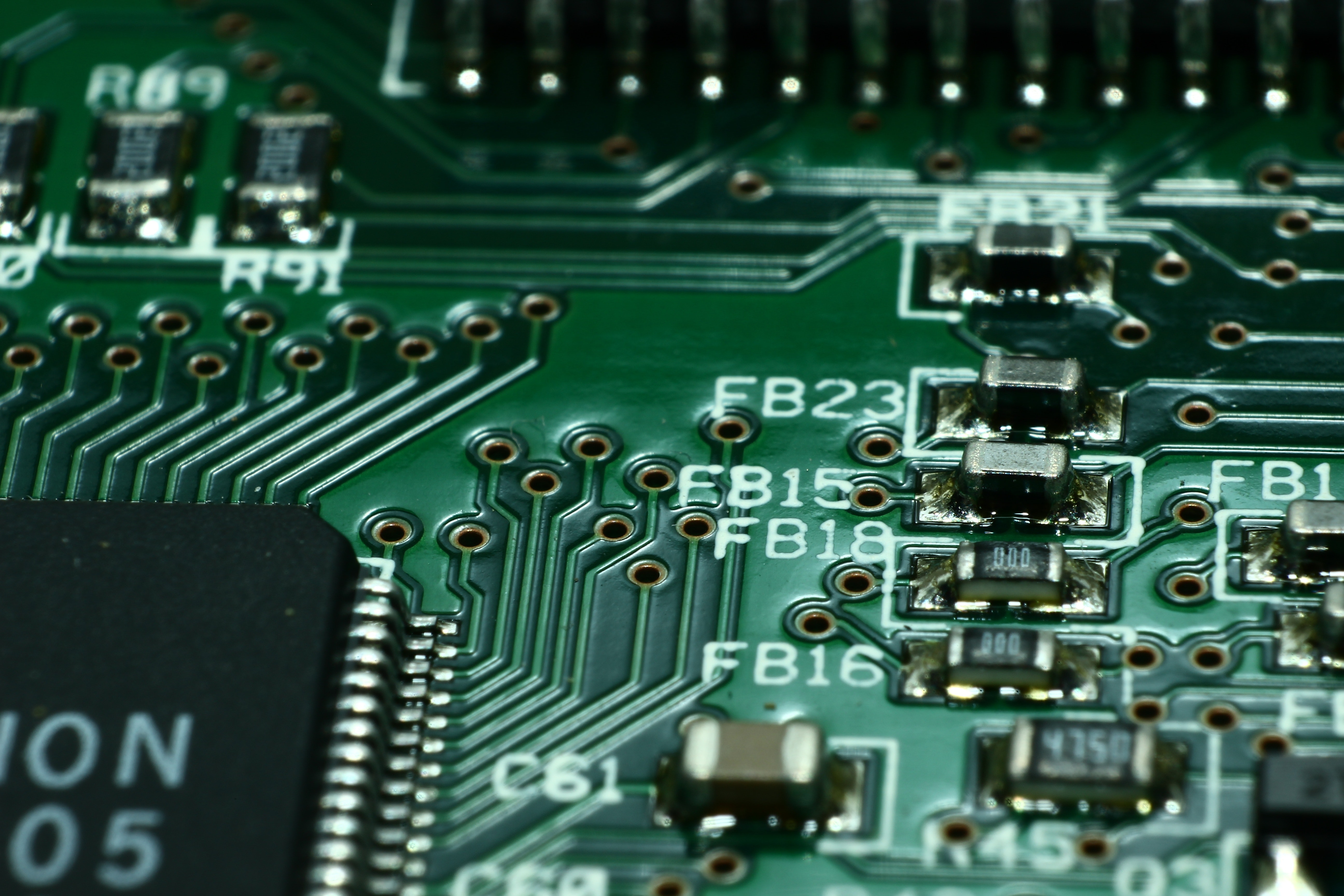
Printed circuit board (PCB) design software helps in designing electronic circuits. The PCB design process involves the placement and routing of components to define electrical connectivity on a circuit board.
PCBs help establish electrical interconnections between components while providing support for holding components and concrete sets that can be combined into an end product. The design and layout of PCBs affect how a circuit works; consequently, the reliability and performance of a printed circuit board depends on whether it has been designed efficiently.


Types of PCBs
Depending upon the use case, one of the following six types of PCBs will be implemented.
-
Single-sided or single-layer PCB: This is the most commonly used PCB board that is easy to design and manufacture. It consists of fixed electrical components on one side of the board while the entire circuit is carved on the other side.
Single-sided PCBs are used for low-cost electrical devices such as LED lighting boards, calculators, FM radios, and timing circuits. - Double-sided or double-layer PCB: This type of circuit board has components on both sides. Double-sided PCBs have a thin layer of conducting material attached to both the top and bottom sides of the board. Metal parts in the board are joined from one side to the other by carving out holes. This type of PCB is applied for power monitoring, cell phone systems, test equipment, amplifiers, etc.
- Multilayer PCB: This category consists of boards with three or more conductive layers that transmit electrical signals between components. Multiple double-sided conductive layers, divided by an equivalent number of insulating material sheets, should be bonded and laminated collectively under high temperatures and pressure. This is to ensure that there are no air gaps and the final PCB assembly is completely stable. Multilayer PCBs are utilized in mobile devices, computers, laptops, tablets, medical equipment, GPS trackers, and various other complex circuits and devices.
- Rigid PCBs: As the name suggests, rigid PCBs are inflexible—these cannot be bent or twisted. Depending on the requirements, it can be single-sided, double-sided, or multilayer but cannot be modified once manufactured. These PCBs are used in X-rays machines, heart monitors, CAT scans, MRI systems, GPS equipment, computers, laptops, tablets, mobile devices, and more.
- Flex PCBs: Flexible or flex PCBs do not include rigid materials. These PCBs are made using the same components as rigid PCBs. However, the core difference is that the board is designed to bend to the required form throughout the application. Depending on the needs, these PCBs may be single-sided, double-sided, or multilayer. Flex PCBs are employed in LCD fabrication, flex solar cells, mobile phones, automotive industries, cameras, organic light emitting diode (OLED) fabrication, and electronic devices such as laptops and computers.
- Rigid-flex PCBs: Rigid-flex PCBs represent a hybrid combination of a rigid and a flex PCB. The most basic form of a rigid-flex PCB comprises a rigid circuit board joined to a flexible circuit board. A rigid-flex board can be folded or constantly flexed and is usually shaped into a curve during manufacturing. Employing flexible PCBs for interconnections removes the requirement for heavy and complex connectors, making the rigid-flex PCBs lighter in weight. Designing this kind of board may be more complicated as these are constructed in 3D, allowing the board to be folded in the desired form for the product. Since these are lightweight and can be designed in 3D format, rigid-flex PCBs are a great fit for various applications across the medical, aerospace, and consumer electronics fields.
Benefits of using PCB design software
Electrical engineers and designers can derive several benefits from PCB design tools as mentioned below:
- Reduces production costs: Using software for designing helps save money on physical models. Virtual designing of the board allows manufacturers to test and verify the design before ordering a prototype for use. It simplifies the design process, saving time and resources.
- Reduces design errors: PCB design software consists of automated checks for detecting errors, identifying compatibility issues, and verifying electrical and physical design rules. It helps in highlighting errors at every step of the designing process, enabling users to rectify those and quickly move to the production stage. It also assists the user in verifying the final PCB design against the original layout for conformity.
- Reduces complications in designing: Designing a PCB is a complex process involving several elements that need to be considered for optimizing the design process. The software enables users to design circuits on boards with various components while removing complications. It assists in speeding up the design process by allowing users to easily change, manipulate, and update the design.
- Lowers production time and time to market for new products: Availability of a user-friendly interface and electrical templates in the software package enhances production time and the time to market for new products. Designers can experiment with the placement of electronic components within the circuit board in a 3D environment to create a favorable design.
PCB design software best practices
In order to make PCB design software work, an organization must adhere to the following best practices:
- Create a schematic: It is important to create a circuit design and schematic using the software tools available. The tool should allow the user to simulate and test the circuit. Having at least one project replica is useful to ensure the circuit will function properly.
- Find the most efficient way of designing PCBs: After testing the circuit design and replica, it is beneficial to find a simple and efficient method of producing PCBs. This can be done after exploring the solutions provided by different manufacturers for designing the boards.
- Verify the design: To save resources, it is important to cross-check the design and board layout for errors.

Anindita Sengupta
Anindita is a Senior Research Analyst at G2 specializing in cloud technologies, CAD & PLM software, and web hosting services. With over five years of experience in market research, Anindita has a proven track record of tracking, analyzing, sizing, and forecasting the industrial printer and B2B software markets. Her passion for technology and staying up-to-date with the latest software trends makes her an invaluable asset to B2B buyers and sellers of software. When she's not immersed in market research, Anindita loves to read and explore new destinations, constantly fueling her curiosity and creativity.


